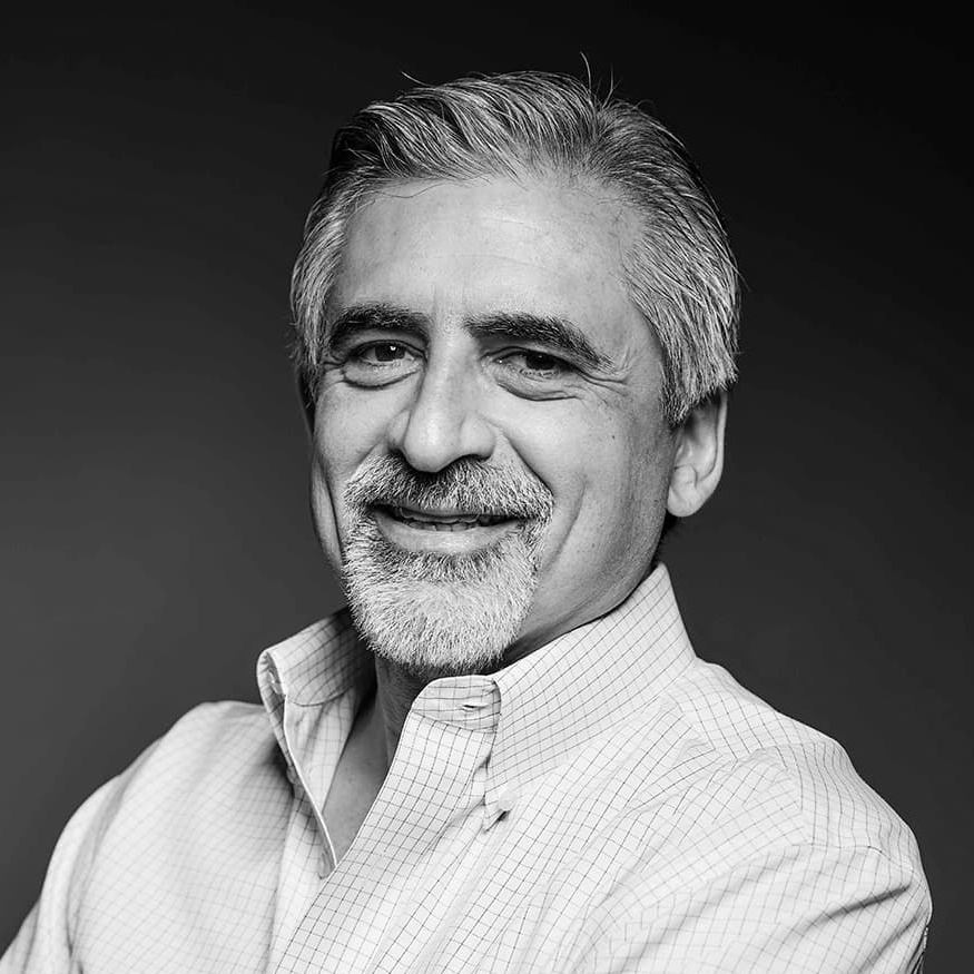
Mo Steinman
Senior Vice President and General Manager, US at Lightelligence, a silicon photonics and optical computing company.
2
APPEARANCES
2
PODCASTS
Oct 14, 2026


Mo SteinmanGUEST
You know, it's racks and racks and racks of servers, and each CPU, each server is a couple of CPUs, some memory DIMMs, you know, maybe a GPU accelerator and some storage and network adapters, and you repeat that a gazillion times, right? There's an observation, uh, that some of the, the hyperscalers have made and published work about, is that if you sort of provision each individual server node, maybe for the worst case or more than the typical case, in average, you're gonna have underutilized resources.
Mo SteinmanGUEST
And particularly if you kind of zoom in on memory, you know, how much memory do you provision in a, in a server? And then multiply that server, you know, m- many, many times in the data center.
Mo SteinmanGUEST
You're very likely to have unused memory, right? And now with the memory shortage, memory is a very expensive commodity, and, you know, if you were a data center operator and somebody told you that 30% of your memory is unused, you'd be pretty mad because you overspent a lot, a lot of money.
Mo SteinmanGUEST
So- The approach to composability is now let's, let's strip down, uh, each individual server node to sort of, like, modest, uh, resources.

Mo SteinmanGUEST
the electronic die needs power and ground connections to the package it also has you know io interfaces like pci express and i squared c and you know rom interface that sort of thing so all of that stuff needs to get to the chip package which is underneath the photonic chip and so you know one way to get that connection is to use wire bonds from the, you know, electronic die to the, or, you know, from either of the die to the package.
Mo SteinmanGUEST
So we have the electronic chip top, directly controlling and interfacing to the photonic die, but also we have through silicon vias, TSVs, going through the photonic die to provide the power and ground connection to the package and to the system to the electronic die sitting above, and also, you know, the I-O connection, you know, the bus interfaces.
Sean BuckleyHOST
Another development from Light Intelligence is the photo wave optical communication hardware that's focused on disaggregated AI memory applications compatible with PCIe 5.0, 6.0, CXL 2.0, and 3.0. Let's explore those a little bit.