Fin field-effect transistor
9
MENTIONS
5
EPISODES
5
PODCASTS
Search complete. 9 mentions across 5 episodes found for "Fin field-effect transistor".
Sep 12, 2026

speaker_1HOST
For a long time, the semiconductor industry relied on relatively flat two-dimensional chip architectures.
speaker_1HOST
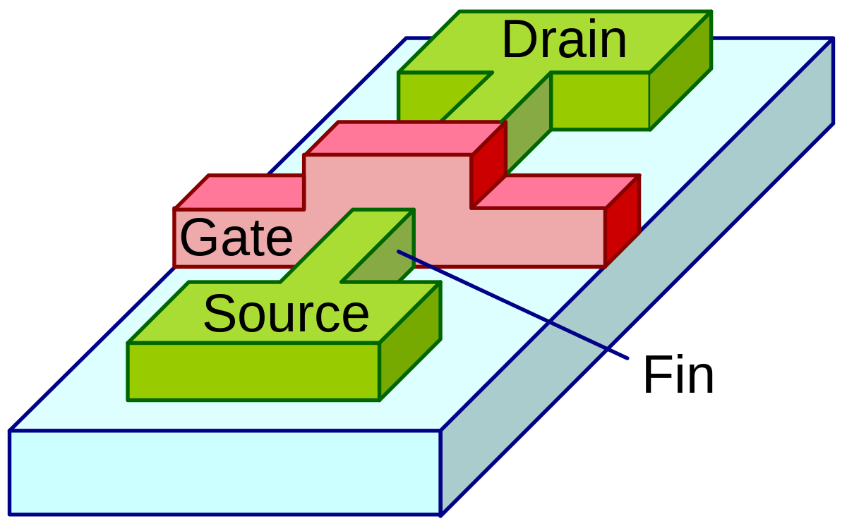
The classic workhorse example is the FinFET.
speaker_0HOST
Okay, the FinFET.
speaker_1HOST
Yeah, you can visualize it as just a flat grid of transistors built directly onto a thick foundational block of bulk silicon.
speaker_0HOST
Okay, so because it's spread out horizontally and sitting on a big solid chunk of silicon, the heat generated by those electrical signals actually has somewhere to go.
speaker_1HOST
And looking ahead to the immediate future, SIAVET's complementary field effect transistors.
speaker_1HOST
Instead of laying components out side by side, engineers are now stacking N-type and P-type transistors directly on top of each other.
speaker_0HOST
So it's almost like, well, if the old FinFET chips were a sprawling single-story neighborhood built right on top of cool, solid dirt, if a house got hot, the heat just sank straight into the earth.

speaker_0HOST
TSMC is suddenly fighting for its absolute life.
speaker_0HOST
They launched these massive corporate espionage lawsuits, throwing an army of lawyers at Samsung to try and slow Liang down, claiming he stole trade secrets regarding their FinFET technology.
speaker_1HOST
But you can't litigate your way to a faster microchip.
speaker_0HOST
Right.

MattHOST
What TSMC have had to do is...
MattHOST
They've had to abandon the transistor design that basically powered the M1 through to the M5, which was a process known as FinFET, which we'll chat a bit about now.
MattHOST
And they've replaced it with this completely new 3D structure called GAFET, which is Gate All Around Field Effect Transistor.
MattHOST
And basically they've achieved this using these nanosheets.

Jim HandyGUEST
I wouldn't count on that as something that would help a shortage.
Jim HandyGUEST
But MRAM is gaining in popularity for a different reason, and that's because when you go to these shrinking processes, you know, 14 nanometers and smaller, they're all FinFET-based, and you can't make NORFLASH on a FinFET.
Jim HandyGUEST
And most microcontrollers have some amount of NORFLASH in them.
Jim HandyGUEST
And so any microcontroller that you want to use one of these advanced processes on, you know, typically a very elaborate microcontroller, is going to need some other kind of memory or an external memory for its, because it can't use Norflash for code storage.